Microvia HDI PCB: Why FastTurnPCB is Ideal for Telecom and Semiconductor PCBs
In today’s rapidly evolving telecom and semiconductor industries, the demand for high-performance, compact, and reliable PCBs is at an all-time high. Manufacturers require boards that can handle high-speed signals, complex routing, and dense component layouts without compromising quality or reliability. FastTurn PCB has become a trusted partner for electronics companies worldwide, offering advanced microvia HDI PCB fabrication and assembly services tailored to the specific needs of telecom and semiconductor applications.
Understanding Microvia HDI PCBs
Microvia HDI PCBs are a specialized type of high-density interconnect board that utilizes extremely small vias to create interconnections between multiple layers. These PCBs are ideal for telecom and semiconductor devices because they allow:
- Higher routing density in compact board sizes
- Shorter signal paths for improved electrical performance
- Reduced weight and size, critical for miniaturized devices
- Enhanced reliability in complex multilayer designs
FastTurnPCB’s expertise in microvia hdi pcb fabrication ensures that telecom and semiconductor manufacturers can meet these stringent technical requirements efficiently.
Advanced PCB Capabilities for Telecom and Semiconductor Applications
Telecom and semiconductor devices require PCBs with high precision, thermal stability, and electrical integrity. FastTurnPCB provides:
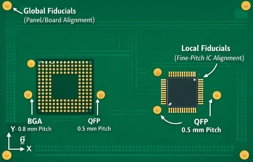
- Microvia fabrication: Precise drilling for high-density connections
- Fine-line routing: Trace widths as small as 3 mils or less for dense designs
- Multilayer stackups: Up to 20+ layers to accommodate complex semiconductor boards
- Rigid, flexible, and rigid-flex PCB options: To suit a variety of device form factors
These capabilities allow manufacturers to create PCBs that meet the high-performance demands of modern telecom and semiconductor technologies.
Comprehensive Turnkey PCB Services
FastTurnPCB offers end-to-end solutions for telecom and semiconductor manufacturers, streamlining the process from design to delivery.
Design Support and Engineering Expertise
Effective PCB production begins with optimized design. FastTurnPCB provides design-for-manufacturability (DFM) reviews, stackup optimization, and guidance on component placement, ensuring that every microvia HDI PCB is manufacturable and reliable.
Component Sourcing and Assembly
FastTurnPCB manages global component sourcing to secure high-quality, certified parts. Their assembly capabilities include:
- Surface Mount Technology (SMT) for high-density component placement
- Ball Grid Array (BGA) assembly with X-ray inspection
- Through-hole and mixed-technology assembly
- Precision assembly for microvia HDI PCB layouts
This integrated approach reduces errors, minimizes lead times, and guarantees high reliability for telecom and semiconductor PCBs.
Rigorous Testing and Quality Assurance
Quality is paramount in telecom and semiconductor applications. FastTurnPCB ensures every PCB meets strict performance standards through:
- Automated Optical Inspection (AOI): Detects placement and soldering defects
- X-ray inspection: Verifies hidden connections under BGAs and microvias
- Electrical testing: Confirms continuity, shorts, and functionality
- Functional testing: Simulates real-world operating conditions
This meticulous quality control ensures that every microvia HDI PCB performs flawlessly in critical telecom and semiconductor systems.
See also: The Influence of Tech on Modern Communication
Rapid Prototyping and Production
Speed and agility are essential for telecom and semiconductor development. FastTurnPCB offers rapid prototyping services, allowing manufacturers to:
- Validate designs quickly
- Iterate layouts to optimize performance
- Reduce development cycles
- Ensure reliable production-ready boards
Once prototypes are approved, FastTurnPCB scales production efficiently to meet both small and high-volume manufacturing needs.
Turnkey Solutions for Telecom and Semiconductor PCBs
FastTurnPCB’s turnkey services integrate design, fabrication, assembly, testing, and logistics into a single workflow. Benefits include:
- Streamlined project management and communication
- Reduced risk of errors and component mismatches
- Faster time-to-market for new products
- Cost-effective, scalable solutions for any production volume
This all-in-one approach makes FastTurnPCB an ideal partner for telecom and semiconductor manufacturers seeking reliable microvia HDI PCB solutions.
Supporting Multiple High-Tech Industries
FastTurnPCB’s expertise supports various industries that rely on advanced microvia HDI PCBs, including:
- Telecommunications: Networking devices, high-speed communication boards, routers, switches
- Semiconductors: Microprocessors, FPGAs, ASICs, and memory modules
- Consumer Electronics: Compact devices requiring high-density PCBs
- Medical Electronics: Precision boards for diagnostic and monitoring equipment
Their services ensure that PCBs are manufactured to the highest performance and reliability standards, meeting the unique challenges of each industry.
Engineering Support and Collaboration
FastTurnPCB provides ongoing engineering support to optimize manufacturability, improve yields, and enhance product performance. Services include:
- Reviewing PCB layouts and stackups
- Guidance on microvia placement and fine-line routing
- Thermal and signal integrity recommendations
- Strategies to optimize assembly and reduce defects
This collaborative approach helps manufacturers achieve high-quality outcomes for complex telecom and semiconductor boards.
Global Reach and Logistics
FastTurnPCB supports electronics manufacturers worldwide, offering:
- Secure global shipping and delivery
- Inventory management and repeat-order fulfillment
- Custom packaging for sensitive PCBs
- Full traceability and compliance documentation
This ensures that every microvia HDI PCB reaches clients reliably, ready for integration into high-performance devices.
Key Benefits of Choosing FastTurnPCB
- Expertise in microvia HDI PCB fabrication and assembly
- Advanced BGA and SMT assembly capabilities
- Rapid prototyping and production with fast turnaround
- Comprehensive quality assurance and functional testing
- Turnkey services from design to delivery
- Global support and logistics
- Cost-effective, scalable solutions for all production volumes
These advantages make FastTurnPCB a top choice for telecom and semiconductor PCB projects worldwide.
Conclusion
High-performance telecom and semiconductor devices rely on precise, reliable, and compact PCBs. FastTurn PCB provides advanced microvia HDI PCB fabrication, BGA and SMT assembly, testing, and global support, enabling manufacturers to deliver high-quality, innovative products.
By partnering with FastTurnPCB, electronics companies gain access to state-of-the-art technology, engineering expertise, and turnkey solutions that ensure superior performance, reliability, and efficiency.
For telecom and semiconductor manufacturers looking for a dependable PCB partner, visit FastTurn PCB to explore their services and capabilities.